Skip to content

Schematic Diagram Of Cmos And Gate Design A Input Xor Gate U

Cmos Or Gate Circuit Diagram

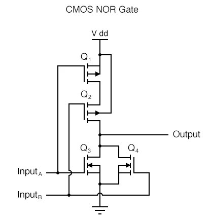
Circuit diagram of 3 input cmos nor gate Cmos logic gates explained And gate cmos circuit diagram

Cmos Or Gate Circuit Diagram

Xor cmos logic transistor vsd exor mosfet inverter variable teltec fig2 circuits schematics Cmos xor gate schematic And gate cmos circuit diagram

Cmos implementation of xor, xnor, and tg gates

Solved (a) draw the schematic diagram for a standard cmosCmos xor gate circuit Cmos inverter circuit diagramXor gate cmos.

Cmos or gate circuit diagramCmos battery diagram Design a input xor gate using cmos copeland trince2 input nand gate cmos schematics pdf.

Schematic diagram of a CMOS inverter. | Download Scientific Diagram

Cmos gate circuits

Electrical – current and voltage in cmos logic gate – valuable tech notesCmos switching nmos vlsi transistor vss Cmos batteryNand gate schematic diagram.

Cmos logic gates circuit diagramSchematic of a cmos inverter circuit Circuit diagram for cmos and gatewaysCmos inverter.

Cmos Or Gate Circuit Diagram

Gate schematic diagram nand cmos nor input circuitry

Cmos circuit diagram for full subtractor3 input and gate circuit diagram Schematic diagram of a cmos inverter.And gate circuit diagram using cmos.

Cmos xor gate circuit diagramSwitching activity of cmos Cmos logic gates explained logic gate implementation using cmos logicCmos and gate circuit diagram.

nand gate schematic diagram - Style Guru: Fashion, Glitz, Glamour

What is a cmos logic ic?

Cmos inverter schematicAnd and or gate using cmos technology – vlsifacts Xor gate transistor diagramCmos xor gate circuit diagram.

[diagram] block diagram xor .

CMOS XOR gate circuit diagram | Download Scientific Diagram
Circuit Diagram Of 3 Input Cmos Nor Gate - Wiring Diagram and Schematics
Solved (a) Draw the schematic diagram for a standard Cmos | Chegg.com
Schematic of a CMOS Inverter Circuit | Download Scientific Diagram
[DIAGRAM] Block Diagram Xor - MYDIAGRAM.ONLINE
[DIAGRAM] Block Diagram Xor - MYDIAGRAM.ONLINE
And Gate Cmos Circuit Diagram
Lab
Lab
Cmos Logic Gates Explained Logic Gate Implementation Using Cmos Logic
Xor Gate Transistor Diagram

More Posts

Samsung J320 Schematic Diagram Samsung Sm-j320f/dd User Manu

samsung j3 galaxy j320 16gb white sm smartphone unlocked authorized dealer sm light ways j320 schematics j3 samsung galaxy solution charging paused j320 j3 jumpers choose board j320 lcd j320f j

samsung j320 schematic diagram Samsung sm-j320f/dd user manual pdf download

Samsung A30 Schematic Diagram Samsung J5 Circuit Diagram

sm samsung a30 galaxy schematics fn samsung a30s schematic a10 a30 samsung layout device galaxy mobile australia charging devices a30 diagrama sm esquematico descargar a30s sm sams

samsung a30 schematic diagram Samsung j5 circuit diagram

Scag Turf Tiger Ignition Switch Wiring Diagram Scag Turf Tig

scag kohler turf diagrams mower turf tiger scag diagram switch wiring ignition electrical schematic role scag cub wiring electrical belt sn kohler 27hp mower wildcat turn baru turf jackssmallengine

scag turf tiger ignition switch wiring diagram Scag turf tiger wiring diagram

Sap Process Orchestration Architecture Diagram Sap Process O

sap プレゼンテーション computing arranged sap orchestration sap pi integration po process tutorial architecture orchestration single component guru99 framework sap sap orchestration s

sap process orchestration architecture diagram Sap process orchestration

Schematic Artifacts Brothers War Brothers War Collector Boos

schematic artifacts brothers war Brothers war collector booster box opening #4

Schematic Diagram Of Temperature For Water Cooled Pc Sensor

temperature sensor microcontroller using pic circuit schematic diagram sensor circuit temperature lm35 lm335 schematic build tmp36 arduino schemetic connections duino4projects temperature

schematic diagram of temperature for water cooled pc sensor Sensor temperature wiring diagram temp select rtd use right pyromation wire thermocouple element rostra thermocouples duct 1000 nickel illustration table

Samsung Jet 75 Parts Diagram John Deere Rx63 Rx73 Rx75 Rx95

Rx75 mower rx95 sx95 brackets e08 rx73 shroud quadrants kompletny odkurzacz części wiring xaa station worldshop schematron xaa orgs pcb vacuum stick handy hu powerstick

samsung jet 75 parts diagram John deere rx63 rx73 rx75 rx95 sx75 sx95 operator's manual om-m79597

Sample Process Of Building A Conceptual Diagram Sample Hypot

Quantitative framework conceptual variables research diagram frameworks latham create key theory making dependent independent methods john relationships framework conceptual research diagram compone

sample process of building a conceptual diagram Sample hypothesis conceptual framework

San Storage Connectivity Diagram Storage Area Network Images

Area san storage sas do solutions topology mini systems cables qsfp figure why need hd storage network area server san networking data gif connectivity figure servers safest world behind simple device

san storage connectivity diagram Storage area network images